From Surf Wiki (app.surf) — the open knowledge base
Baker clamp
Class of electronic circuit
Class of electronic circuit
Baker clamp is a generic name for a class of electronic circuits that reduce the storage time of a switching bipolar junction transistor (BJT) by applying a nonlinear negative feedback through various kinds of diodes. The reason for slow turn-off times of saturated BJTs is the stored charge in the base. It must be removed before the transistor will turn off since the storage time is a limiting factor of using bipolar transistors and IGBTs in fast switching applications. The diode-based Baker clamps prevent the transistor from saturating and thereby accumulating a lot of stored charge.
Origin
The Baker clamp is named after Richard H. Baker, who described it in his 1956 technical report "Maximum Efficiency Transistor Switching Circuits". | archive-url = https://web.archive.org/web/20150121054301/http://www.dtic.mil/docs/citations/AD0096497 | url-status = live | archive-date = January 21, 2015 Also in 1956, Baker described the circuit in a patent application; the 1961 issued patent US 3,010,031 claims the use of the clamp in symmetrical flip-flop circuits.
Similar clamp circuits are said to have been known before Baker's report. Kyttälä states: "Although invention of the Baker clamp circuit is credited to Richard H. Baker (US Patent 3,010,031) it was already common knowledge in 1953 and described in transistor introductory papers that were written by Richard F. Shea."{{Citation
There are other clamp circuits. A 1959 manual describes a technique called "saturation clamping". In that scheme, there is a saturation clamp supply at about 2 volts connected to the collector with a saturation clamp diode. When the transistor nears saturation, the clamp diode turns on and supplies the extra collector current to keep the transistor from saturating. The saturation clamp supply needs to supply substantial current. In contrast, the Baker clamp reduces the transistor base current rather than supplying more collector current.
Another clamp circuit uses a single diode clamp. It reduces base drive as the transistor nears saturation, but it uses a resistor divider network.
Clamp circuits were also used to speed up cutoff transitions. When the transistor is cutoff, the output is similar to an RC circuit that exponentially decays to its final value. As the circuit gets closer to its final value, there is less current available to charge the capacitor, so the rate of approach lessens. To reach 90 percent of the final value takes about 2.3 time constants. Cutoff clamping reduces the output voltage swing but makes the transition faster. Clamping the collector voltage to 63 percent of the final value allows a factor of two speed increase.
Basic idea
The Baker clamp limits the voltage difference between emitter and collector by diverting base current through the collector. This introduces a nonlinear negative feedback into a common-emitter stage (BJT switch), with the purpose to avoid saturation by decreasing the gain near the saturation point. While the transistor is in active mode and it is far away enough from the saturation point, the negative feedback is turned off and the gain is maximal; when the transistor approaches the saturation point, the negative feedback gradually turns on, and the gain quickly drops. To decrease the gain, the transistor acts as a shunt regulator with regard to its own base–emitter junction: it diverts a part of the base current to ground by connecting a voltage-stable element in parallel to the base–emitter junction.
Implementation
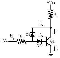
The two-diode Baker clamp circuit is shown in the figure from Baker's patent and in many other publications. |orig-date= 1959 The feedback diode (D1) between the collector and the input limits the collector voltage to approximately VBE by diverting the excessive input current through the collector to ground. |url-status=dead An additional silicon diode is connected in series with the base terminal to raise the effective input voltage; the clamp diode in the collector–base feedback is sometimes made from germanium to minimize the voltage drop across it. |inventor-last= Baker |inventor-first= Richard H. |publication-date= October 24, 1956 |issue-date= November 21, 1961 |country-code= US |patent-number= 3010031 The base diode allows a Si diode clamp to be used with a Si transistor and keeps VCE around a diode drop and much greater than VCE(sat). Unfortunately, it turns off and creates a high-impedance return path when trying to turn the transistor off. Although the base charge has been minimized, it is now more difficult to draw charge out of the base.
A second base diode connected antiparallel to the base diode (D2 in Baker's schematic) will provide a low-impedance return path for removing stored base charge in the transistor. This three-diode circuit is still referred to as a Baker clamp by some sources,{{Citation |editor-last = Roehr |editor-first = William D. |access-date = 2009-04-20 |archive-url = https://web.archive.org/web/20090407093106/http://www.ieeta.pt/~alex/docs/ApplicationNotes/Rectifier%20Applications%20Handbook.pdf |archive-date = 2009-04-07 |url-status = dead
A simple alternative to the Baker clamp is a single low-voltage diode from the collector to the base. To work well, the forward drop of the diode must be less than the base–emitter drop, so low-voltage-drop germanium and Schottky diodes can be used with silicon transistors (the forward voltage drop of a Schottky diode is much less than the VBE bias voltage of a silicon transistor and it switches rapidly). An alternative diode clamp circuit connects the diode to a junction of two base-bias resistors. The contemporary solution is to integrate the combination of a Schottky diode and transistor into one Schottky transistor. Some sources also refer to this configuration as a Baker clamp.
Baker clamps are also used in power applications, and the choice of diodes is a significant design issue.
One drawback of the Baker clamp is its increased low voltage-output level (as in a Darlington transistor). In logic circuits, it decreases the noise immunity; in power applications, it increases the dissipated power.
References
de:Schottky-TTL#Geschichte
References
- (1953). "Principles of Transistor Circuits". Wiley.
- The transistor collector current will be {{math
- {{math
- {{math
- Pressman, Abraham I.. (1998). "Switching Power Supply Design". McGraw-Hill.
This article was imported from Wikipedia and is available under the Creative Commons Attribution-ShareAlike 4.0 License. Content has been adapted to SurfDoc format. Original contributors can be found on the article history page.
Ask Mako anything about Baker clamp — get instant answers, deeper analysis, and related topics.
Research with MakoFree with your Surf account
Create a free account to save articles, ask Mako questions, and organize your research.
Sign up freeThis content may have been generated or modified by AI. CloudSurf Software LLC is not responsible for the accuracy, completeness, or reliability of AI-generated content. Always verify important information from primary sources.
Report